- 您现在的位置:买卖IC网 > Sheet目录1992 > DAC5674IPHPG4 (Texas Instruments)IC DAC 14BIT 400MSPS 48-HTQFP
DAC5674
SLWS148A SEPTEMBER 2003 REVISED OCTOBER 2005
www.ti.com
25
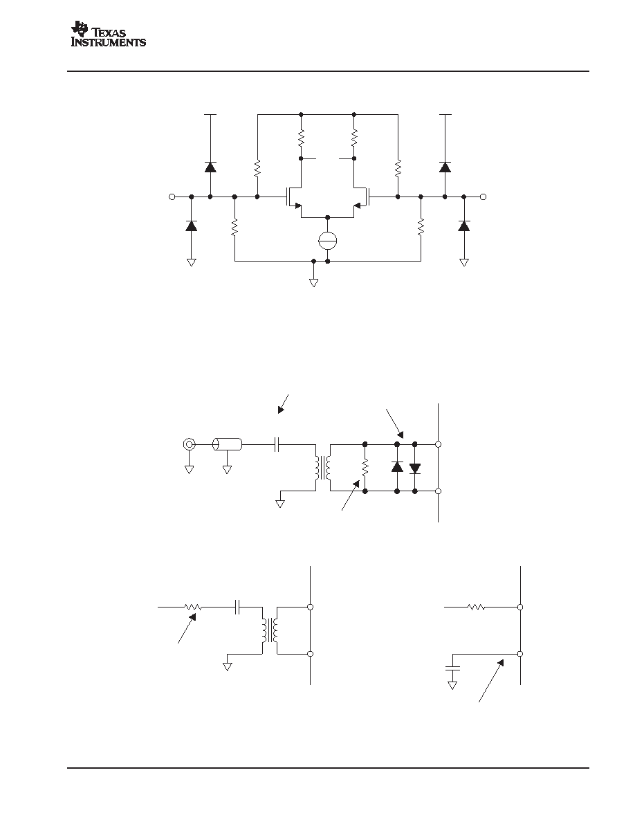
Figure 29 shows an equivalent circuit for the clock input.
CLK
Internal
Digital In
CLKC
CLKGND
R1
10 k
AVDD
R1
10 k
R2
10 k
R2
10 k
AVDD
CLKVDD
Figure 29. Clock Input Equivalent Circuit
Figure 30, Figure 31, Figure 32, and Figure 33 show various input configurations for driving the differential
clock input (CLK/CLKC).
RT
200
CLK
1:4
CLKC
Termination Resistor
Swing Limitation
Optional, May Be Bypassed
for Sine Wave Input
CAC
0.1
F
Figure 30. Preferred Clock Input Configuration
Ropt
22
CLK
1:1
CLKC
Optional, Reduces
Clock Feedthrough
CAC
0.01
F
TTL/CMOS
Source
Ropt
22
CLK
CLKC
Node CLKC
Internally Biased
to IVDD 2
TTL/CMOS
Source
0.01
F
Figure 31. Driving the DAC5674 With a Single-Ended TTL/CMOS Clock Source
发布紧急采购,3分钟左右您将得到回复。
相关PDF资料
DAC7621EBG4
IC SNGL 12BIT PARALLEL D/A 20SSO
DAC7801KPG4
IC DUAL 12BIT CMOS DAC 24-DIP
DAC8043AESZ
IC DAC 12BIT MULT SRL INP 8SOIC
DAC8043GP
IC DAC 12BIT MULTIPLY CMOS 8-DIP
DAC8221GP
IC DAC 12BIT DUAL W/BUFF 24-DIP
DAC8222GPZ
IC DAC 12BIT DUAL W/BUFF 24DIP
DAC8229FSZ-REEL
IC DAC 8BIT DUAL V-OUT 20SOIC
DAC8248FS
IC DAC 12BIT DUAL W/BUFF 24-SOIC
相关代理商/技术参数
DAC5674IPHP-ND
制造商: 功能描述: 制造商:undefined 功能描述:
DAC5674IPHPR
功能描述:数模转换器- DAC 14-Bit 400 CommsDAC RoHS:否 制造商:Texas Instruments 转换器数量:1 DAC 输出端数量:1 转换速率:2 MSPs 分辨率:16 bit 接口类型:QSPI, SPI, Serial (3-Wire, Microwire) 稳定时间:1 us 最大工作温度:+ 85 C 安装风格:SMD/SMT 封装 / 箱体:SOIC-14 封装:Tube
DAC5674IPHPRG4
功能描述:数模转换器- DAC 14-Bit 400 CommsDAC RoHS:否 制造商:Texas Instruments 转换器数量:1 DAC 输出端数量:1 转换速率:2 MSPs 分辨率:16 bit 接口类型:QSPI, SPI, Serial (3-Wire, Microwire) 稳定时间:1 us 最大工作温度:+ 85 C 安装风格:SMD/SMT 封装 / 箱体:SOIC-14 封装:Tube
DAC5675
制造商:TI 制造商全称:Texas Instruments 功能描述:14-BIT, 400-MSPS DIGITAL-TO-ANALOG CONVERTER
DAC5675A
制造商:TI 制造商全称:Texas Instruments 功能描述:14-Bit, 400MSPS Digital-to-Analog Converter
DAC5675AEVM
功能描述:数据转换 IC 开发工具 DAC5675A Eval Mod RoHS:否 制造商:Texas Instruments 产品:Demonstration Kits 类型:ADC 工具用于评估:ADS130E08 接口类型:SPI 工作电源电压:- 6 V to + 6 V
DAC5675AIPHP
功能描述:数模转换器- DAC 14-Bit 400-MSPS RoHS:否 制造商:Texas Instruments 转换器数量:1 DAC 输出端数量:1 转换速率:2 MSPs 分辨率:16 bit 接口类型:QSPI, SPI, Serial (3-Wire, Microwire) 稳定时间:1 us 最大工作温度:+ 85 C 安装风格:SMD/SMT 封装 / 箱体:SOIC-14 封装:Tube
DAC5675AIPHP
制造商:Texas Instruments 功能描述:IC DAC 14BIT 400MSPS 48-HTQFP